 RF
RF
1-Bit and 4-Bit Comparator Design in Verilog
This article presents Verilog HDL code for designing 1-bit and 4-bit comparators, including truth tables and simulation results.
Showing 25 posts (Page 1 of 2)
Advertisement
This article presents Verilog HDL code for designing 1-bit and 4-bit comparators, including truth tables and simulation results.

Verilog HDL code for a 2 to 4 decoder implementation, truth table, and simulation results.

Verilog source code for a 32-bit Arithmetic Logic Unit (ALU) capable of performing arithmetic and logical operations. Includes truth table and simulation results.
Verilog code for a 4-bit BCD asynchronous reset counter, including module definition and reset functionality.
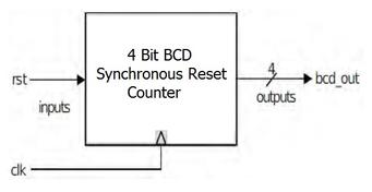
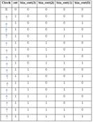
Verilog source code for a 4-bit BCD synchronous reset counter, block diagram, and truth table for understanding its operation.
Verilog code implementation of a 4-bit binary asynchronous reset counter, including block diagram and truth table.
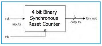
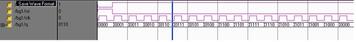
Verilog code for a 4-bit binary synchronous reset counter, complete with a block diagram and truth table for understanding its operation.
Verilog implementation of a 4-bit binary to Gray code counter converter with symbol, truth table, and simulation results.
Verilog code for a 4-bit down counter is presented, along with its corresponding test bench for simulation and verification.
Verilog code for a 4-bit Mod 13 counter with its test bench, including explanations of the code's functionality.

Verilog HDL code for a 4-to-1 multiplexer and a 1-to-4 demultiplexer, including truth tables and simulation results.

Verilog HDL code for an 8-to-1 multiplexer, including its symbol, truth table, and simulation results.
Verilog source code for an 8-to-3 encoder without priority, including a block diagram and truth table for understanding its functionality.

Verilog code for an 8-to-3 priority encoder, including the truth table, schematic, code explanation, and simulation results.
Verilog code for an 8-to-3 priority encoder, complete with a block diagram and truth table for understanding its functionality.
Learn about asynchronous FIFO design for reliable data transfer between independent clock domains. Includes Verilog code, block diagrams, and test bench.

Explore a D flip-flop implementation without reset, including Verilog code, test bench, simulation results, and RTL schematic.

Explore the Verilog code, test bench, simulation, and RTL schematic of a D flip-flop with synchronous reset.
Explore the FPGA job market, essential skills (VHDL, Verilog), top hiring companies, and expected salary ranges for FPGA engineers.
Explore FPGAs: their architecture with CLBs, advantages like reprogrammability and speed, applications in embedded systems, development tools, and VHDL/Verilog coding steps.

Verilog HDL implementation of a full adder, including truth table, code, and simulation results.

Explore Verilog implementations of Mealy and Moore state machines, highlighting the differences in their output logic.
Verilog code and test bench for a parallel load shift left register, including explanations of the code's functionality.
Verilog code for a PRBS generator and its test bench are presented, explaining the linear feedback shift register (LFSR) implementation.

Explore Verilog code implementations for RAM (Random Access Memory) and ROM (Read Only Memory) with detailed examples and figures.
Advertisement