 RF
RFSISO vs. SIPO vs. PISO vs. PIPO: Shift Register Types
Advertisement
This article clarifies the distinctions between SISO, SIPO, PISO, and PIPO shift registers. In a shift register, each clock pulse shifts the register’s contents by one bit to the right or left. The serial input determines what data enters the leftmost flip-flop during the shift. We’ll compare 4-bit SISO, SIPO, PISO, and PIPO shift registers.
In an ‘n-bit’ register, ‘n’ clock pulses are needed to serially enter ‘n’ bits of data. Shift registers are commonly used in DSP-based algorithms because each shift left corresponds to multiplying the data by 2, and each shift right corresponds to dividing the data by 2.
SISO (Serial In Serial Out) Shift Register
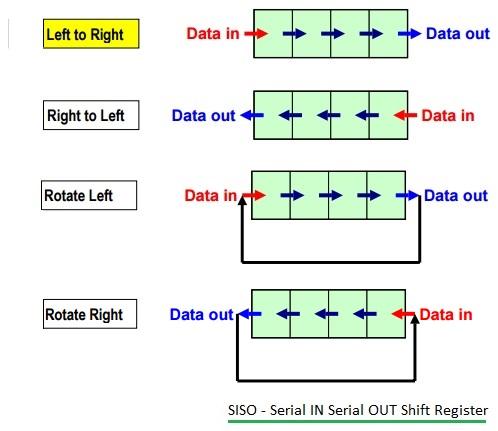
Figure 1 illustrates a SISO shift register.
There are four types of SISO registers:
- Shift left without rotate
- Shift right without rotate
- Shift left with rotate
- Shift right with rotate
In a right-shift SISO register, the Least Significant Bit (LSB) data is applied to the Most Significant Bit (MSB) flip-flop (e.g., a D flip-flop). SISO registers can introduce a delay equivalent to ‘n’ clock pulses to the input data. If ‘T’ is the time period of one clock pulse, the total delay provided by SISO is ‘n*T’. In a left-shift SISO register, the MSB data is applied to the LSB flip-flop (D flip-flop).
- Clock pulses needed for input: n
- Clock pulses needed for output: n
PIPO (Parallel In Parallel Out) Storage Register
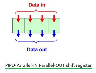
Figure 2 shows a PIPO register.
The PIPO type is a storage register built from D flip-flops. It isn’t strictly a shift register.
- Clock pulses needed for parallel input data: 1
- Clock pulses needed for parallel output data: 0
SIPO (Serial In Parallel Out) Shift Register
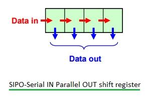
Figure 3 illustrates a SIPO shift register.
-
For storing ‘n’ bits of serial input data, ‘n’ clock pulses are required.
-
For storing ‘n’ bits of parallel output data, zero clock pulses are required, as no clock pulse is needed for this operation.
-
Clock pulses needed for input: n
-
Clock pulses needed for output: 0
PISO (Parallel In Serial Out) Shift Register
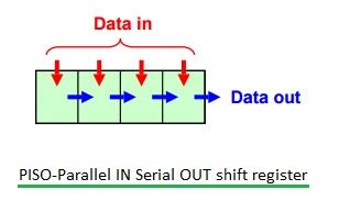
Figure 4 illustrates a PISO shift register.
-
It is a parallel data storage register. To store ‘n’ bits, one clock pulse is needed.
-
To provide serial data as output, ‘(n-1)’ clock pulses are needed.
-
Clock pulses needed for input: 1
-
Clock pulses needed for output: n-1
Advertisement


