Emitter Coupled Logic (ECL) Circuits Explained
Advertisement
Emitter-Coupled Logic (ECL) is a digital logic family that uses bipolar junction transistors (BJTs) for its implementation. Unlike CMOS (Complementary Metal-Oxide-Semiconductor), which uses both n-type and p-type MOSFETs, ECL relies on bipolar transistors.
ECL is known for its high-speed operation but consumes higher power compared to CMOS.
Key Characteristics of ECL Circuits
ECL circuits typically use differential amplifier pairs, composed of multiple transistors, as the basic building blocks. The differential pairs are used to create logic gates and flip-flops.
In ECL, multiple transistors are connected in such a way that their emitters are coupled together. This creates a differential pair that forms the basis of logic gates. The differential pairs amplify the voltage difference between two inputs. This characteristic makes ECL circuits less susceptible to noise and provides high-speed operation.
ECL circuits often use a constant current source to bias the transistors. This helps maintain a consistent operating point and ensures a fast response time.
Let us explore ECL logic circuits for various gates, which include the ECL inverter, ECL NAND and AND gates, and ECL NOR and OR gates.
ECL Inverter

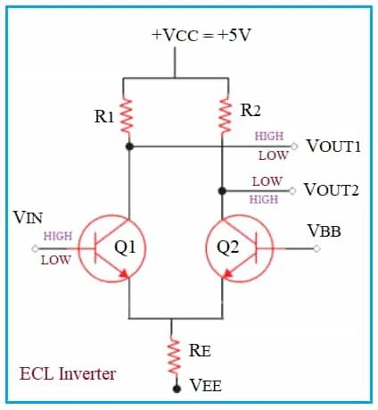
In ECL circuits, an inverter is typically implemented using a pair of transistors in a differential amplifier configuration. As shown in the figure above, the ECL inverter circuit consists of two transistors: an transistor (Q1) and a transistor (Q2). The emitters of Q1 and Q2 are commonly connected, forming a differential pair.
The input signal is applied to the base of the transistor (Q1). A reference voltage (usually derived from a voltage divider) is applied to the base of the transistor (Q2).
Let us understand the working of the ECL inverter circuit. The differential pair operates in such a way that when the input voltage is high, the transistor (Q1) is turned on, allowing current to flow through the emitter resistor. At the same time, the transistor (Q2) is turned off due to the lower voltage at its base.
The emitter current of Q1 (Ie1) flows through the emitter resistor, generating a voltage drop. This voltage drop creates a voltage difference between the common emitter node and the reference voltage. The voltage difference at the common emitter node is used as the output voltage.
The output voltage is typically pulled down to a low level (logic 0) when the input voltage is high. The differential pair and the emitter resistor act as a current-steering arrangement. The voltage difference at the common emitter node causes a current to be steered towards one of the transistors, determining the logic state of the output.
Case-1: When Vin = HIGH, Q1 transistor = ON, Q2 transistor = OFF, VOUT2 is pulled to 5 V through R2, VOUT1 = 4.2 V (LOW) as the voltage drop across R1 is 0.8V. VE = VOUT1 – VQ1 => 4.2V – 0.4V = 3.8V (as transistor Q1 is turned ON completely).
Case-2: When Vin = LOW, Q2 transistor is ON and Q1 transistor is OFF. Hence VOUT1 is pulled to 5.0 V through the R1 resistor. Here VOUT2 = 4.2 V. Also VE -> VOUT2 – VQ2 -> 4.2V – 0.8V -> 3.4V as transistor Q2 is turned ON.
ECL NAND Gate

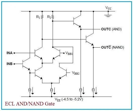
An ECL NAND gate is constructed using multiple transistors to achieve the logic functionality. The basic structure involves differential pairs and additional transistors for signal inversion and combination. As shown in the figure above, two differential pairs are used, each receiving one of the inputs (A and B).
Additional transistors are connected to the collectors of the differential pairs to form a logical AND function. The outputs of these transistor stacks are then combined to produce the NAND gate’s final output. The final output is typically taken from an emitter-follower stage, which provides a low-impedance output for driving subsequent stages.
ECL NOR Gate

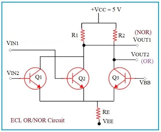
Similarly, an ECL NOR gate is constructed using differential pairs and additional transistors to achieve the logical NOR function. As shown in the figure above, two differential pairs receive the inputs (A and B). Additional transistors are connected to the collectors of the differential pairs to form a logical OR function. The outputs of these transistor stacks are then combined to produce the NOR gate’s final output. The output is typically taken from an emitter-follower stage for a low-impedance output.
Advantages and Disadvantages of ECL
The advantages of ECL logic families are as follows:
- High-speed operation: ECL circuits are known for their fast switching speeds.
- Differential signaling: Reduces susceptibility to noise.
The disadvantages of ECL circuits are as follows:
- Higher power consumption: Compared to CMOS.
- Limited fan-out: Due to the current-steering nature of ECL.
- Requires careful control of operating conditions: For optimal performance.
Conclusion
In summary, ECL circuits use bipolar transistors and differential signaling to achieve high-speed digital logic operations. While they offer advantages in terms of speed, they are generally less power-efficient than CMOS and are often used in applications where speed is a critical factor.
Advertisement
 RF
RF


