MOSFET Fabrication: A Step-by-Step Guide
Advertisement
This document outlines the fabrication steps involved in creating MOS devices, specifically focusing on the MOSFET (Metal-Oxide-Semiconductor Field-Effect Transistor). Let’s break down the process:

Fabrication Steps for NMOS Transistors
The fabrication of an NMOS transistor involves several key steps. These include:
1. SiO2 Layer Formation
The process begins with a p-type silicon (Si) substrate. A silicon dioxide (SiO2) layer is formed on the surface of this substrate. This is achieved by exposing the top surface of the silicon to dry oxygen. This oxidation process creates a thin, insulating layer of SiO2.
2. n+ Layer Diffusion
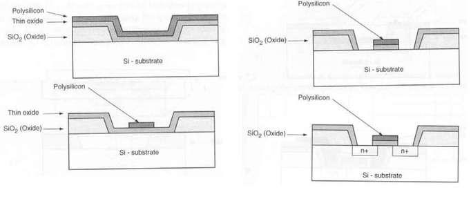
Next, two heavily doped n-type (n+) regions are created within the p-type substrate. This is done through a diffusion process. Openings are created using photo-resist and ultraviolet (UV) lithography. The n-type dopants are then diffused into the silicon through these openings, forming the source and drain regions.
3. Photoetching
In this step, the central part of the SiO2 layer is selectively removed using masking and photoetching techniques. This exposes the area where the gate will be formed.
4. Re-oxidation
The entire top surface of the structure is now exposed to dry oxygen once again. This leads to the formation of a new SiO2 layer that completely covers the top surface, including the area where the gate oxide was previously removed. This layer serves as the gate insulator.
5. Deposition
A layer of phosphosilicate glass (PSG) is deposited over the entire surface of the SiO2 layer. This PSG layer helps to protect the underlying layers and can also act as a diffusion source in later processing steps.
6. Photoetching (Again!)
Using UV lithography, two more windows are opened in the SiO2 layer. These windows are located directly above the n+ diffused regions (source and drain). These openings are essential for making electrical contact to the source and drain.
7. Metallization
The entire top surface of the device is then metalized using aluminum (Al). This metal layer provides a conductive path for electrical signals.
8. Masking and Etching (Final Touch)
Finally, the aluminum metal is patterned using masking and photoetching. The unwanted metal is etched away, leaving behind the metal contacts to the gate, drain, and source regions. This defines the final electrical connections of the MOSFET.
The figure above visually represents this NMOS MOSFET fabrication process. Each step is crucial in creating a functional transistor.
Advertisement
 RF
RF


