Power Supply Noise Reduction Techniques: Basics and Types
Advertisement
This article covers the basics of power supply noise reduction techniques and mentions different types of techniques used.
Power Supply Noise Sources
The following are common power supply noise sources in PCB circuits:
- Location, width, and length of power supply traces and ground traces on the board. Improper routing can introduce inductance and impedance, leading to noise.
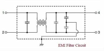
- Multi-stage EMI filters are not used for AC and DC supply portions on the board. Lack of filtering allows noise to propagate into the circuit.
- Bypassing and decoupling capacitors are not used at appropriate places on the PCB circuit which is interfaced with the power supply lines. Insufficient decoupling can cause voltage fluctuations and noise.
- Use of improper earth coupling and grounding techniques on the board. Poor grounding creates ground loops and increases noise susceptibility.

Power Supply Noise Reduction Techniques
Here are some of the most common power supply noise reduction techniques:
-
Use of bypass capacitors to reduce noise current on the power supply lines. Bypass high derivative sinks and sources with appropriate capacitors as per desired frequencies. Avoid formed lead capacitors. Ceramic capacitors are good for high frequencies.
-
Use of decoupling to isolate two circuits on a common line. This is used to prevent the transmission of noise from one circuit to the other circuit. A common decoupling network is a low pass filter. Choose a low value and low-Q series inductor in the filter.
-
Increase the mutual coupling between the paths. This is achieved by increasing the width and decreasing the distance between them. Place the forward path and return path as close as possible.
-
In two layer boards, use a power grid with a ground plane. This reduces self-inductance and is commonly applied to digital board design. In analog boards, an appropriate C dec tree structure is used to minimize length and inductance.
-
Identify high derivative current sources and sinks and their return paths. All these need to be bypassed. For the total board, 10 mA/µS is an ideal limit for max. di/dt.
-
During PCB layout design, place the forward path as close to the return path as possible. Maximize trace width to minimize inductance. Avoid long supply traces and layout supply busses in grid or plane.
-
Bypass capacitors are used at appropriate places in feed-forward amplifier circuits. Op-Amps are quite sensitive to noise on the power supply. Hence, op-amp circuits should be appropriately designed to reduce the effect of noise.
-
Use multistage EMI filters to reduce power supply noise to the PCB circuit design.
Advertisement
 RF
RF


