 RF
RF74HC595 Shift Register IC and pin diagram
Advertisement
The 74HC595 is a popular integrated circuit (IC) used as a shift register in digital electronics. It belongs to the 74HC family of ICs, which are widely used in various applications due to their compatibility with TTL (Transistor-Transistor Logic) and CMOS (Complementary Metal-Oxide-Semiconductor) logic levels.
Let’s delve into the 74HC595 shift register circuit, explore the 74HC595 pin diagram, and understand its specifications and features. The 74HC595 is commonly used when you need to expand the number of output pins of a microcontroller or drive multiple LEDs, displays, or other digital components using fewer pins from the microcontroller. Its serial-in, parallel-out nature makes it efficient for driving multiple outputs while conserving resources.
74HC595 Pin Diagram
The figure below and the accompanying table detail the pins of the 74HC595.
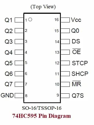
The 74HC595 is an 8-bit serial-in, serial or parallel-out shift register. This means it can store and shift 8 bits of data serially (one bit at a time) into its internal registers and then output these bits either serially or in parallel.
Like most ICs, the 74HC595 requires a stable power supply voltage, typically in the range of 2 to 6 volts.
| Pin number | Description |
|---|---|
| 1 | Q1, Parallel data output-1 |
| 2 | Q2, Parallel data output-2 |
| 3 | Q3, Parallel data output-3 |
| 4 | Q4, Parallel data output-4 |
| 5 | Q5, Parallel data output-5 |
| 6 | Q6, Parallel data output-6 |
| 7 | Q7, Parallel data output-7 |
| 8 | GND Ground |
| 9 | Q7S, Serial data output |
| 10 | MR’ (Master Reset Input) |
| 11 | SHCP, Shift Register Clock Input |
| 12 | STCP, Storage Register Clock Input |
| 13 | OE’ (Output Enable Input) |
| 14 | DS, Serial Data Input |
| 15 | Q0, Parallel Data Output-0 |
| 16 | Vcc, Supply Voltage |
The Q0-Q7 pins are the parallel output pins. They hold the current state of the data stored in the shift register. These outputs reflect the serial data shifted in or the data loaded in parallel based on the state of the shift register.
The 74HC595 also features a storage register that latches the data from the shift register when the latch enable (STCP) pin is pulsed. This latched data then appears at the output pins (Q0-Q7).
The output enable (OE’) pin controls whether the outputs are enabled or disabled.
Clock Signals
The 74HC595 utilizes two clock signals:
- Serial Clock (SHCP): This clock signal controls the shifting of data into the shift register.
- Latch Clock (STCP): This clock signal controls the transfer of data from the shift register to the storage register and subsequently to the output pins.
74HC595 Shift Register Circuit
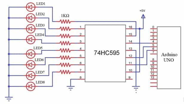
The 74HC595 shift register is often interfaced with Arduino microcontrollers for controlling multiple LEDs because it provides a convenient way to expand the number of output pins available on the Arduino board. It is commonly used in such applications, as shown in the figure above.
Applications of 74HC595
Here are some common applications of the 74HC595:
- Serial to Parallel data conversion
- To capture and hold data for an extended period of time.
- General purpose logic
- Allow simple serial bit streams from a microcontroller to control as many peripheral lines as required.
- Wide array of products such as appliances, computer peripherals, industrial control, and so on.
Conclusion
Overall, the 74HC595 shift register IC offers a versatile and efficient solution for expanding the output capabilities of microcontroller platforms like Arduino. Its ability to store and output data serially enables the control of multiple LEDs or other digital components using a minimal number of GPIO pins.
Advertisement


