 RF
RFADC DAC Interfacing with FPGA using VHDL
Advertisement
This page describes ADC DAC interfacing with FPGA. The ADC VHDL Code is used to read data from ADC to receive. The DAC VHDL code is used to write data to DAC for transmit.
Introduction
As shown in Figure 1, a 12-bit ADC and a 14-bit DAC are interfaced with an FPGA. The FPGA uses 16 I/O pins to interface the ADC/DAC for parallel and fast read/write access.
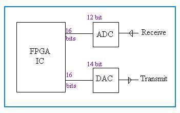
An ADC converts an analog signal into digital data format. The ADC VHDL code for the receiver part is mentioned below, where 12 bits are converted to 16 bits with four leading zeroes for the FPGA to read the digital data from the ADC.
ADC DAC Interface Pin Diagram
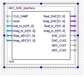
Figure 2 depicts the ADC DAC interface pin diagram for both the receive and transmit sections.
The DAC VHDL code for the transmit side can also be coded similarly to the ADC VHDL code mentioned below, with slight modifications.
ADC VHDL Code
library IEEE;
use IEEE.STD_LOGIC_1164.ALL;
use IEEE.STD_LOGIC_ARITH.ALL;
use IEEE.STD_LOGIC_UNSIGNED.ALL;

entity adc_dac_interface is
    port (
        CLK_SAMP            : in std_logic;
        reset               : in std_logic;
        enable_in           : in std_logic;
        Real_in_from_ADC    : in std_logic_vector(11 downto 0);  -- receiver side i/p
        imag_in_from_ADC    : in std_logic_vector(11 downto 0);  -- receiver side i/p
        Real_adc_to_phy     : out std_logic_vector(15 downto 0); -- receiver side o/p
        imag_adc_to_phy     : out std_logic_vector(15 downto 0); -- receiver side o/p
        ADC_CLK1            : out std_logic;
        ADC_CLK2            : out std_logic;
        enable_out          : out std_logic
    );
end entity;

architecture beh of adc_dac_interface is
begin
    process(CLK_SAMP, reset)
    begin
        if reset = '1' then
            enable_out <= '0';
            real_adc_to_phy <= (others => '0');
            imag_adc_to_phy <= (others => '0');
        elsif CLK_SAMP = '1' and CLK_SAMP'event then
            real_adc_to_phy <= Real_in_from_ADC(11) & Real_in_from_ADC(11) & Real_in_from_ADC(11) & Real_in_from_ADC(11) & Real_in_from_ADC;
            imag_adc_to_phy <= imag_in_from_ADC(11) & imag_in_from_ADC(11) & imag_in_from_ADC(11) & imag_in_from_ADC(11) & imag_in_from_ADC;
            enable_out <= enable_in;
        end if;
    end process;

    ADC_CLK1 <= CLK_SAMP;
    ADC_CLK2 <= CLK_SAMP;
end beh;
ADC DAC Serial Data Interfacing with FPGA
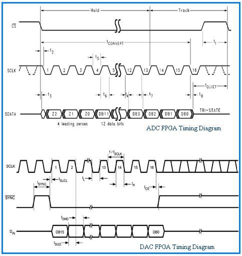
Figure 3 depicts the ADC and DAC serial data interface timing diagram obtained from the datasheets of the ADC/DAC. Both the ADC and DAC are 12-bit analog-to-digital converters and 12-bit digital-to-analog converters, respectively.
In the ADC FPGA interface, CS is pulled low, and then four zeroes are transmitted, followed by 12 bits. These 12 bits represent the voltage acquired by the ADC. The MSB (Most Significant Bit) is clocked first. ADC FPGA VHDL/VERILOG code for the same can be easily written.
In the DAC FPGA interface, SYNC is pulled HIGH, and then 16 bits are written. The first 2 bits are zeroes, the next 2 bits are configuration bits, and the remaining 12 bits are the actual information to be converted to analog format for transmission. DAC FPGA VHDL/VERILOG code for the same can be easily written.
Advertisement


